Introduction
General Product Information
The RT7231 is a high-performance 650kHz 4A step down regulator with an internal power switch and synchronous rectifier. It features quick transient response using its Advanced Constant On-Time (ACOTTM) control architecture that provides stable operation with small ceramic output capacitors and without complicated external compensation, among other benefits. The input voltage range is from 4.5V to 18V and the output is adjustable from 0.765V to 8V.
The proprietary ACOTTM control improves upon other fast response constant on-time architectures, achieving nearly constant switching frequency over line, load, and output voltage ranges. Since there is no internal clock, response to transients is nearly instantaneous and inductor current can ramp quickly to maintain output regulation without large bulk output capacitance. The RT7231 is stable with and optimized for ceramic output capacitors.
With its internal 90mΩ switch and 60mΩ synchronous rectifier, the RT7231 displays excellent efficiency and good behavior across a range of applications, especially for low output voltages and low duty cycles. Cycle-by cycle current limit, input under-voltage lock-out, externally-adjustable soft-start, output under- and overvoltage protection, and thermal shutdown provide safe and smooth operation in all operating conditions.
The RT7231 evaluation board uses the RT7231GQW IC in a WDFN-10L 3x3 package with an exposed thermal pad. The IC is also available in a PTSSOP-14 package with an exposed thermal pad.
Product Feature
- Fast Transient Response
- Steady 650kHz Switching Frequency at All Load
- 4A Output Current
- Advanced Constant On-Time (ACOTTM) Control
- Optimized for Ceramic Output Capacitors
- 4.5V to 18V Input Voltage Range
- Internal 90mΩ Switch and 60mΩ Synchronous Rectifier
- 0.765V to 8V Adjustable Output Voltage
- Externally-adjustable, Pre-biased Compatible Soft-Start
- Cycle-by-Cycle Current Limit
- Output Over- and Under-voltage Shut-down
Key Performance Summary Table
|
Key features
|
Evaluation board number: PCB002_V1
|
|
Default Input voltage
|
12V
|
|
Max Output Current
|
4A
|
|
Default Output Voltage
|
1.05V
|
|
Default Marking & Package Type
|
RT7231GQW (WDFN-10L 3x3)
|
|
Operation Frequency
|
Steady 650kHz at all load
|
|
Other Key Features
|
Advanced constant On-time(ACOTTM) control
Power Good
Adjustable Soft-start (external capacitor)
|
|
Protection
|
Over current protection:
Cycle-by-Cycle Current Limit
Hiccup Mode Output Over- and Under-voltage Shut-down
|
Bench Test Setup Conditions
Headers Description and Placement
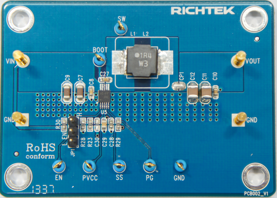
Please carefully inspect the EVB IC and external components, comparing them to the following Bill of Materials, to ensure that all components are installed and undamaged. If any components are missing or damaged during transportation, please contact the distributor or send e-mail to evb_service@richtek.com.
Test Points
The EVB is provided with the test points and pin names listed in the table below.
|
Test point/
Pin name
|
Signal
|
Comment (expected waveforms or voltage levels on test points)
|
|
VIN
|
Input voltage
|
Input voltage range = 4.5V to 18V
|
|
VOUT
|
Output voltage
|
Default output voltage = 1.05V
Output voltage range = 0.765V to 8V
(see ‘’ Output Voltage Setting’’ section for changing output voltage level)
|
|
GND
|
Ground
|
Ground reference for the input voltage, output voltage and analog ground
|
|
SW
|
Switching node test point
|
SW waveform
|
|
EN
|
Enable test point
|
Enable signal. Drive EN or install a shorting block on Jumper JP1 to enable operation (shorting 2-3) or disable operation (shorting 1-2).
|
|
JP1
|
Chip enable control
|
Install jumper or drive EN directly to enable or disable operation
|
|
BOOT
|
Boot strap supply test point
|
Floating supply voltage for the high-side N-MOSFET switch
|
|
SS
|
Soft-start control test point
|
Soft start waveform
|
|
PVCC
|
Linear regulator output test point
|
Internal linear regulator output= 5.1V
|
|
PG
|
Power good output test point
|
Connected to PVCC through R29, PG voltage is 5.1V when soft-start is complete and the output voltage is in regulation
|
Power-up & Measurement
Procedure
1.Connect a jumper at JP1 terminals 1 and 2, connecting EN to GND, to disable operation.
2.Apply a 12V nominal input power supply (4.5V < VIN < 18V) to the VIN and GND terminals.
3.Set the jumper at JP1 to connect terminals 2 and 3, connecting EN to VIN through resistor R30, to enable operation.
4.Verify the output voltage (approximately 1.05V) between VOUT and GND.
5.Connect an external load up to 4A to the VOUT and GND terminals and verify the output voltage and current.
Output Voltage Setting
Set the output voltage with the resistive divider (R23, R28) between VOUT and GND with the midpoint at FB. The output is set by the following formula:
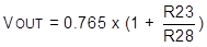
The installed VOUT capacitors (C11, C12) are 22μF, 16V X5R ceramic types. Do not exceed their operating voltage range and consider their voltage coefficient (capacitance vs. bias voltage) and ensure that the capacitance is sufficient to maintain stability and provide sufficient transient response for your application. Installing a small 5pF to 22pF capacitor at C30 (in parallel with R23) may be desirable to improve transient response for higher output voltages. See the RT7231 IC datasheet for more information.
Schematic, Bill of Materials and Board Layout
EVB Schematic Diagram
C7, C9: 10μF/50V/X5R, 1206, TDK C3216X5R1H106K
C11, C12: 22μF/16V/X5R, 1210, Murata GRM32ER61C226K
L1: 1.4μH TAIYO YUDEN NR8040T1R4N, DCR=7mΩ
Bill of Materials
|
Reference
|
Qty
|
Part number
|
Description
|
Package
|
Manufacture
|
|
U5
|
1
|
RT7231GQW
|
DC/DC Converter
|
WDFN-10L 3x3
|
Richtek
|
|
C7,C9
|
2
|
C3216X5R1H106K160AB
|
10μF/±10%/50V/X5R
Ceramic Capacitor
|
1206
|
TDK
|
|
C11,C12
|
2
|
GRM32ER61C226KE20#
|
22μF/±10%/16V/X5R
Ceramic Capacitor
|
1210
|
Murata
|
|
C28
|
1
|
0603B392K500
|
3.9nF/±10%/50V/X7R
Ceramic Capacitor
|
0603
|
WALSIN
|
|
C8,C10,C27
|
3
|
C1608X7R1H104K080AA
|
0.1μF/±10%/50V/X7R
Ceramic Capacitor
|
0603
|
TDK
|
|
C29
|
1
|
C1608X5R1E105K080AC
|
1μF/±10%/25V/X5R
Ceramic Capacitor
|
0603
|
TDK
|
|
C30
|
0
|
|
Not Installed
|
0603
|
|
|
L1
|
1
|
NR8040T1R4N
|
1.4μH/7A/±30%,
DCR=7mΩ, Inductor
|
8mmx8mmx4mm
|
TAIYO YUDEN
|
|
L2
|
0
|
|
Not Installed
|
|
|
|
R28
|
1
|
|
22k/±5%, Resistor
|
0603
|
|
|
R23
|
1
|
|
8.2k/±5%, Resistor
|
0603
|
|
|
R29
|
1
|
|
10k/±5%, Resistor
|
0603
|
|
|
R30
|
1
|
|
100k/±5%, Resistor
|
0603
|
|
|
CP1
|
1
|
|
0 (Short)
|
|
|
|
JP1
|
1
|
|
3-Pin Header
|
|
|
|
TP1/2/3/4/5/6
|
6
|
|
Test Pin
|
|
|
|
GP
|
5
|
|
Golden Pin
|
|
|
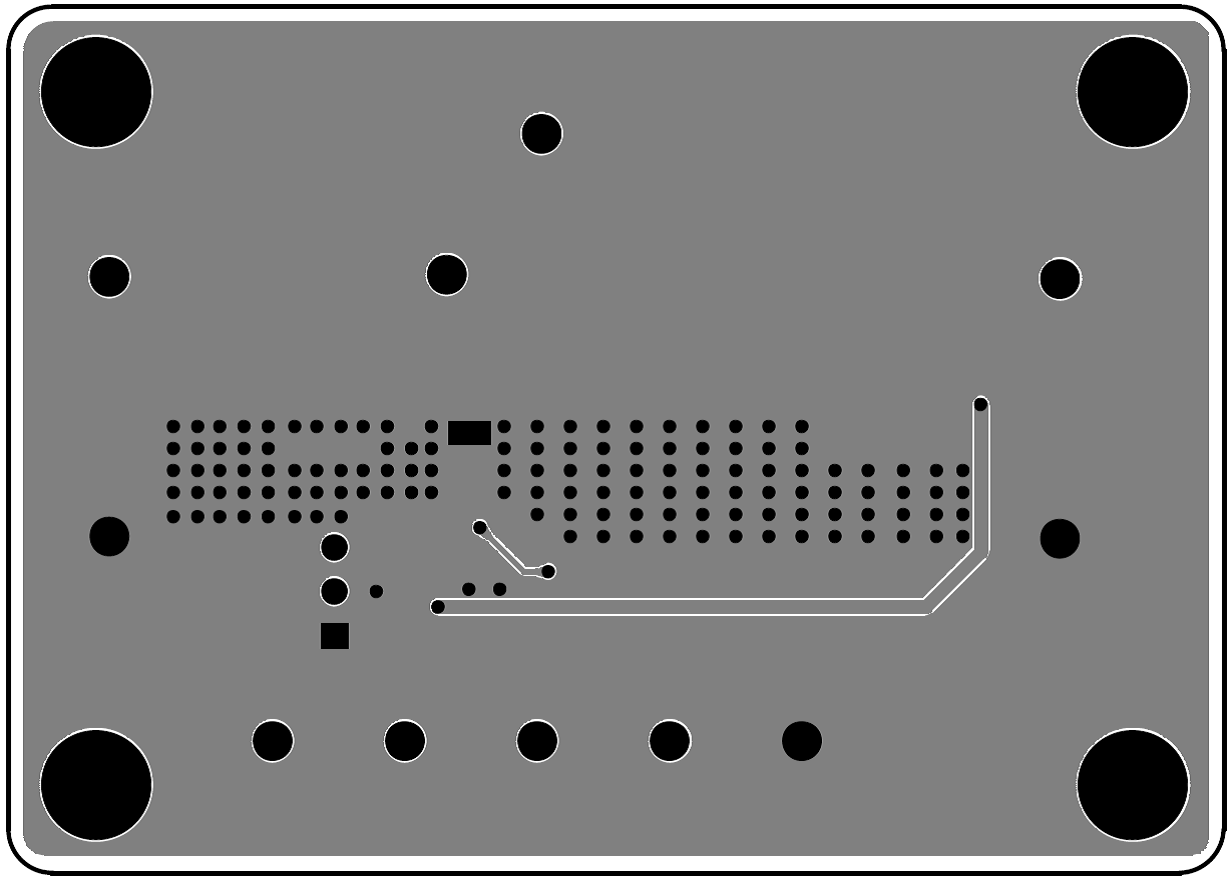
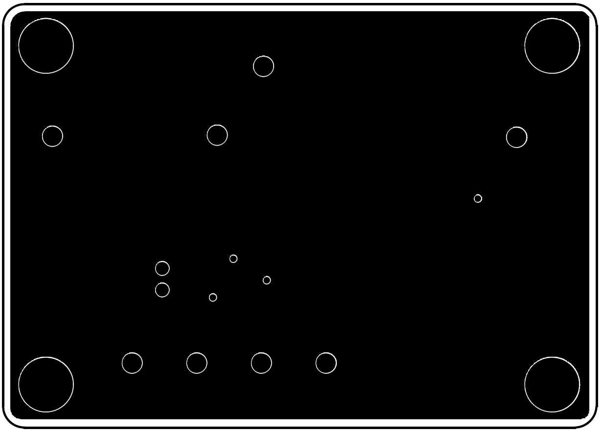
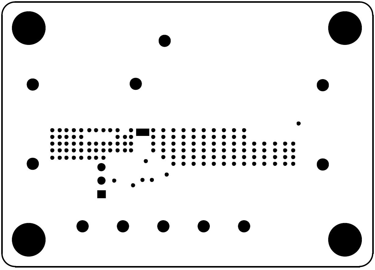
EVB Layout
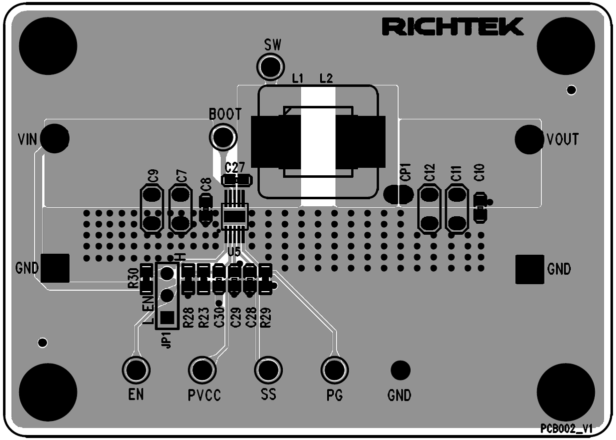
Top View (1stlayer)
Bottom View (4thLayer)
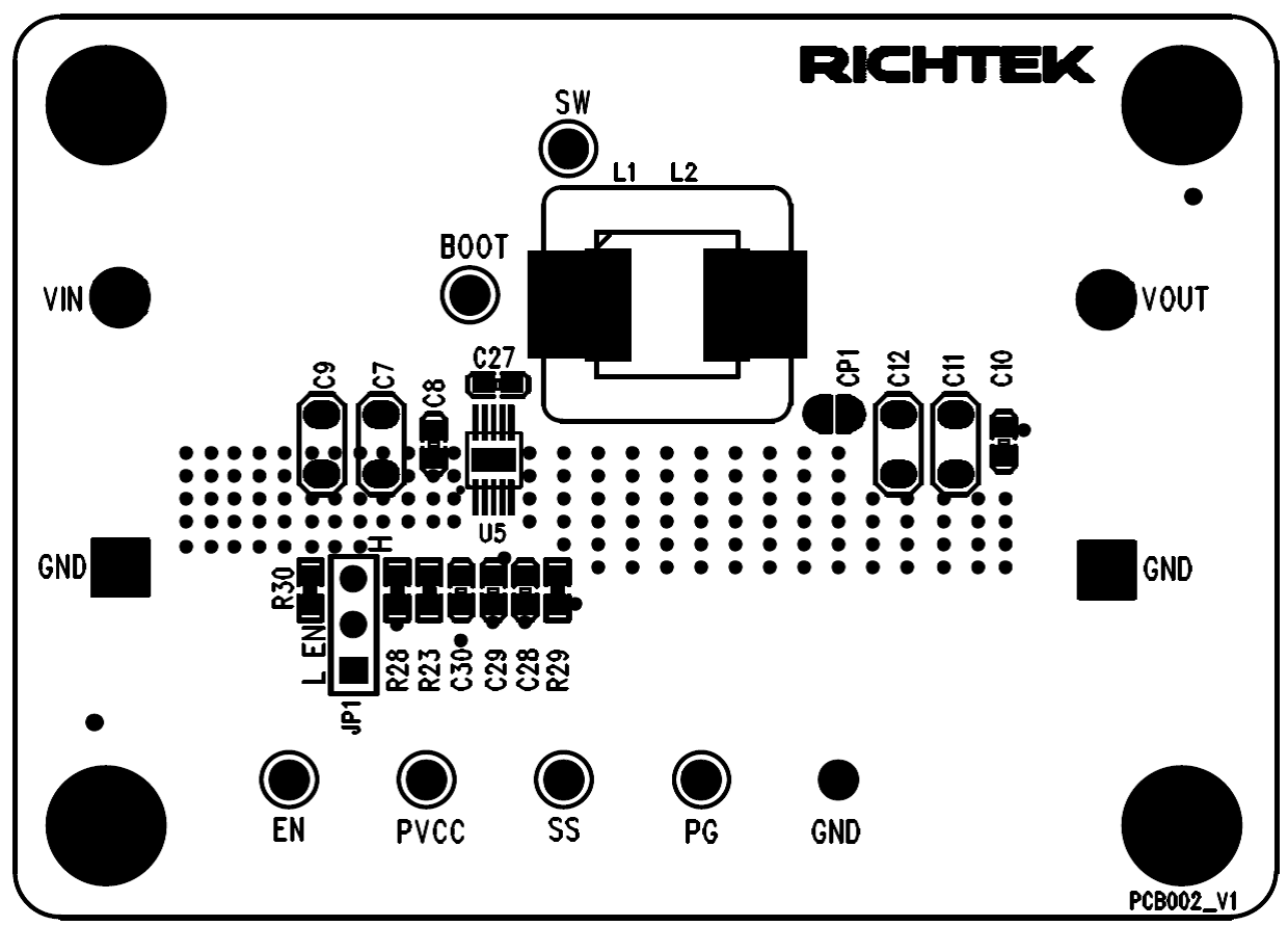
Component Placement Guide—Component Side (1stlayer)
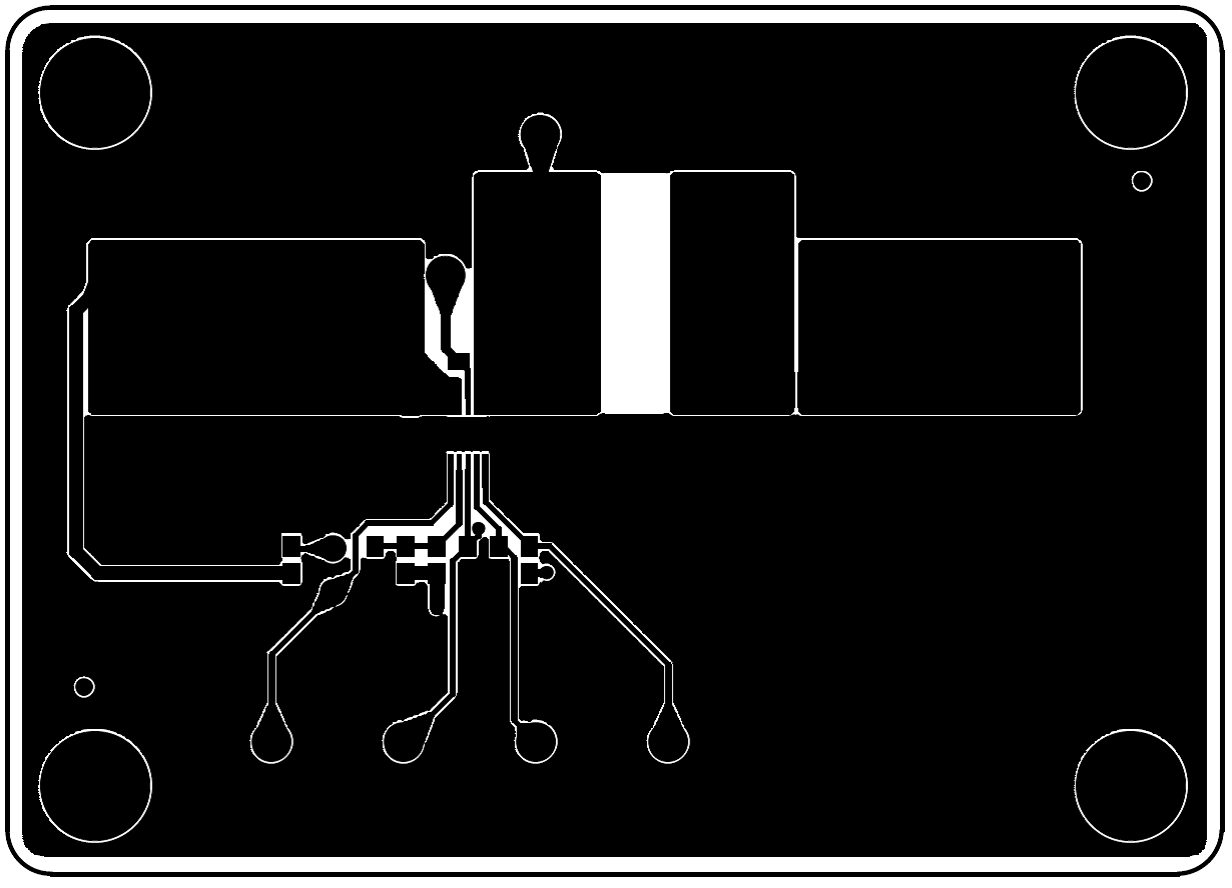
PCB Layout—Component Side (1stLayer)

PCB Layout—Inner Side (2nd Layer)
PCB Layout—Inner Side (3rd Layer)
Component Placement Guide—Bottom Side (4th Layer)
PCB Layout—Bottom Side (4th layer)